About
Introduction
ARISTech was founded by industry experts with more than 10 years of individual experience in the semiconductor field with a focus on innovative technological development.
Based on our rich experience and technological expertise, we have been successful in a variety of semiconductor-related businesses at home and abroad, focusing on developing and producing controller ICs for flash memory storage devices, developing and supporting flash memory technologies, and offering strategic consultation within the semiconductor industry.
During the second half of 2008, we launched our flash memory storage business, including a line of SSDs and flash memory cards based on our cutting edge in-house technology. Today, we are proud to be at the forefront of the industry in flash memory applications through our continued investment in research and development.
As we continue to grow and move forward into an exciting new chapter, our goal is to become a leader in the tech sector by continuing to develop cutting-edge technologies and products backed by a client-centric management policy.
Vision
Striving to follow a client-centric management policy of offering the highest quality product and services, our vision is to offer cutting edge technology and expertise to our clients and partners.
ARISTech’s vision is to become a comprehensive semiconductor company with a focus on innovative technological development with a client-centric approach. To this end, our goal is to develop products from the client’s perspective based on our industry-leading expertise and our core principles of Goodwill, Wisdom, and Hope.
Business History
2002 - 2007 Founding
- 2002.07 Founding of ARISTech Co., Ltd.
- 2002.12 Consultation of semiconductor equipment marketing for local manufacturer
- 2003.08 Consultation of Brazilian semiconductor assembly house on behalf of US corporation
- 2003.12 Commencement of development of flash memory control IC
- 2004.03 Development contract for flash memory control IC with “A” semiconductor company
- 2004.04 Registration of ‘Technology Venture Company’
- 2004.10 Contract for development of flash memory tester with ”B” semiconductor company
- 2005.02 Establishment and increased investment of venture capital
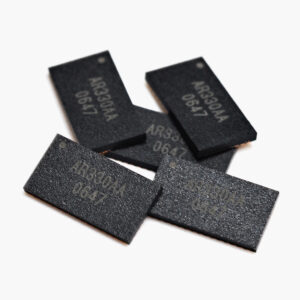
- 2005.04 Development of Flash Memory Control IC (AR300AA, AR310AA) for MMC card
- 2005.06 Contract for development of flash memory control SoC with research institute established by the Korean government
- 2005.09 Release of flash memory control IC (AR300AA, AR310AA) for MMC
- 2006.07 Development contract for flash memory behavioral tester
- 2006.09 Development of flash memory combo Control IC (AR330AA) for SD and MMC cards
- 2006.09 Patent application and registration of semiconductor packaging
- 2007.01 Production of localized Micro SD Card with in-house Control IC and flash memory made in Korea
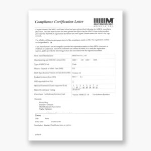
- 2007.02 Acquisition of MMC Certification from MMC Association
- 2007.04 Development of Control IC (AR320A) for microSD
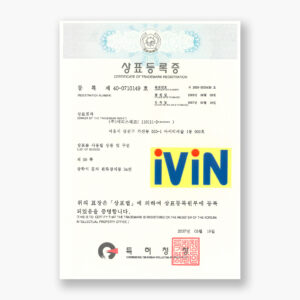
- 2007.05 Trademark registration of ‘iVIN’ for Flash Storage products
- 2007.06 Development of new dual Control IC (AR330BB) for SD and MMC cards

2008 - 2012 Growth
- 2008.02 Establishment of Storage Business Unit in Seongnam
- 2008.05 Commencement of outsourced test business
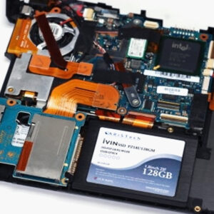
- 2008.12 Development of SSD/UFD
- 2009.03 Sales launch of 2.5” SATA and 1.3” PATA SSD
- 2009.04 Mass production and export of microSD
- 2009.07 Registration and certification of in-house corporate affiliate research institute
- 2009.08 Quality and reliability approval by major local PC manufacturer
- 2009.10 Release of four new SSD models with the world’s fastest speed for 1.8′ ZIF
- 2009.10 Export of UFD at $5M USD
- 2010.02 Certification of Microsoft Window-7 application for SSD products
- 2010.06 Expansion of UFD and SSD sales to Japan
- 2011.06 Delivery of SSD to Daejeon Transportation Corporation
- 2011.08 Delivery of SSD to AMKOR Technology
- 2011.09 Export of UFD and SSD of$10M USD
- 2012.01 Certification of ISO 9001 and ISO 14001
- 2012.12 Trademark registration of ‘mySSD’


2013 - Expansion
- 2013.01 Agreement with Alcor Micro Inc. for technological alliance and sales cooperation
- 2013.03 Launch of two types of network storage devices
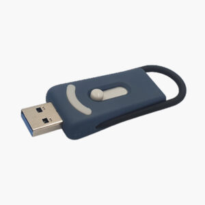
- 2014.06 Launch of OTG-USB flash drives
- 2014.12 Annual revenue of $20M USD
- 2016.06 Acquisition of flash memory recycling technology
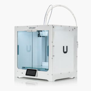
- 2017.01 Implementation of advanced 3D printing systems
- 2018.03 Expansion and relocation of manufacturing facility
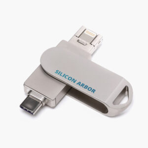
- 2020.02 Launch of newly designed UFD for Amazon
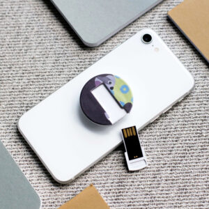
- 2020.08 Development of UFD containing phone grip with proprietary design


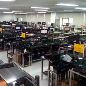
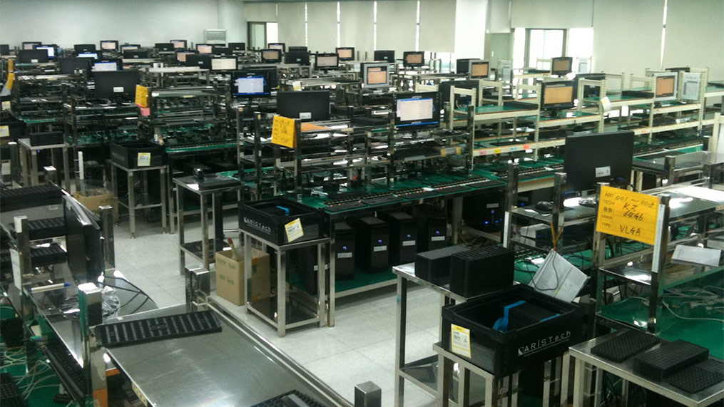
Manufacturing Facility
There is a business using ARISTECH's NAND flash technology. NAND flash memory produced by a semiconductor company is finally classified as good and defective after various test processes. NAND flash memory, which is classified as defective, has various causes. It is divided into a wide variety of types, from structural defects inside semiconductors to poor wire bonding in packages. Therefore, some of these defective products are not a serious problem for consumers to use. For example, 120GB of 128GB capacity is available to be used. ARISTECH has set up a business that re-tests these defective NAND flash memories and classifies them according to quality performance. We have developed simulating boards that simulate the end products that use NAND flash memories, and classified NAND flash memory into several categories. This business enables NAND flash memory manufacturers to generate a certain level of profit from recycling the NAND flash memory.
ARISTech signed a contract with a domestic memory semiconductor company in 2008 and has changed its contents and form so far, but the business is in the same context. We have tested tens of millions of NAND flash memory so far.
Located in Seongnam, the southern part of Seoul, our factory is located close to the customers, enhancing logistics convenience. In terms of testing facilities, it has more than 5,000 NAND memory tests at a time, including decontamination facilities to clean and post-process contaminated packages, re-ball facilities for NAND flash memory packages, laser marking facilities to mark package surfaces, and vision inspectors. In conclusion, we equipped all the facilities and other related machines, and materials to do this kind of business.
The semiconductor IC, which has been in progress so far, is NAND flash memory, and the types of packages are TSOP, VLGA, ULGA, etc., and even chips that are in silicon wafer state are included. It also includes MCP (NAND MEMORY + DRAM), eMMC (NAND MEMORY + MMC CONTROLLER), uMCP (UFS + DRAM), UFS (NAND MEMORY + UFS CONTROLLER), and eMCP (eMMC + DRAM). In addition to these single packages, we also proceed with materials mounted on defective SSD PCBs.